Capabilities

TECHNOLOGIES

We manufacture high quality printed circuit boards. Our manufacturing facilities produce prototypes and full production runs locally & overseas with quality as standard. We provide high quality pcb at a low competitive price.
We have a well-educated & experienced technical team that is very knowledgeable in understanding design. With our experience we are capable of removing any road blocks or issues that could arise during production, if needed and with our customer approval. Our in house engineering department does complete DFM/DRC, including visual checks of your design. Why visual checks? Because DFM & DRC is not always 100% accurate. This will help finding errors and save time & cost.
Our capabilities are wide; we have sources globally to meet almost any kind of PCB requirement. We always work hard to fulfill our customer requests in a cost effective and efficient manner.

PROFESSIONAL SERVICES

CAPABILITIES IN NON-STANDARD PCB PROCESS

  • Finish Types: IMMERSION GOLD (ENIG), IMMERSION SILVER (IAG), WHITE TIN (ISN), OSP, HARD IMM GOLD, GOLD FLASH (SOFT BONDABLE GOLD), BARE COPPER FINISH
  • Material Types: CEM 1 & 3, FR4 – 170 TG (HIGH TG), FR-406, FR-408, ISOLA 410, ROGERS, GETEK, POLYMIDE, ALUMINIUM, NELCO, HALOGEN FREE, FLEX & RIGID-FLEX
  • Board Thickness: 0.010mil, 0.031mil, 0.047mil, 0.093mil, 0.125mil
  • Copper Weight: 4oz & anything over it please email us we will do our best to meet your requirement
  • Mask Type: Matte, Glossy, Semi-Glossy
  • Trace/Spacing: 0.004mil
  • Routing: TAB–ROUTE, V-SCORE & JUMP, TAB-ROUTE-SCORE , CUT-OUTS, CONTROL DEPTH CUT-OUTS
  • Mask Color: variety of colors available for your choice
  • Silk Screen: variety of colors available for your choice
  • Testing: Netlist testing, flying probe and continuity test

CAPABILITIES IN STANDARD PCB PROCESS:

  • Class 2 Fabrication
  • Finish Type: Leaded or Lead-Free
  • Material Type: FR4 (135TG)
  • Board Thickness: 0.062inch
  • Copper Weight: 1oz
  • Trace/Spacing: 0.008mil
  • Routing: Individual
  • Smallest holes size: 0.010mil to 0.015mil
  • Minimum Annual Ring: 0.005mil (each side for plating)
  • Solder Mask: both side (with color green)
  • Component Markings: both side (Silk, with color white)
  • SMT top or bottom side with atleast 0.021mil pitch min

CAPABILITIES IN SPECIAL PCB PROCESS

  • Gold Fingers/Edge Connectors
  • Blind-Vias
  • Di-Electric Thickness
  • Impedance Control
  • Carbon Ink
  • Counter Sink/Counter Bore
  • Edge plating & Beveling
  • Laser drill & Micro Vias
  • BGA
  • VIPO
  • Plugged Vias (Conductive and Non-Conductive Ink)
  • Cut-outs
  • Control Depth Cut-outs and Routing

ADDITIONAL INFO

is cut into laminate (material) it is a “cone” or “Y” shape hole which has a degree in cutting. Counter sink is used for screw head which allows screw to fit flat in laminate. Requirement to drill counter sink hole depend on diameter of the head with degree & depth on laminate surface, diameter of hole size, plated or non-plated, side of the counter sink head (top or bottom).
is just like a regular plated via hole, it connects one external layer to any internal layer of PCB depending on the requirement, but it does not go all the way like through-holes on the board. Buried Via is also just like a regular plated via hole which connects internal layers only and dose not connect to any external layers. Also it does not go all the way like through holes on the board. Blind and buried via technology is used for to meet density of the board design without increasing the layer count and board size.
is cut into laminate (material) it is a “T” shape hole. It has a flat head with no degree to cut in laminate compare to counter sink. Counter bore is used for screw head which allows screw to fit flat in laminate. Requirement to drill counter bore hole depend on diameter of the head, depth of the cut-out in laminate, diameter of the hole size, plated or non-plated, side of the counter bore head (top or bottom).
is a cut in laminate (material). It is used for putting any component which allows it to lay flat in laminate. Requirement for doing control depth cut-out is length and width of cut-out and depth of cut-out in laminate.
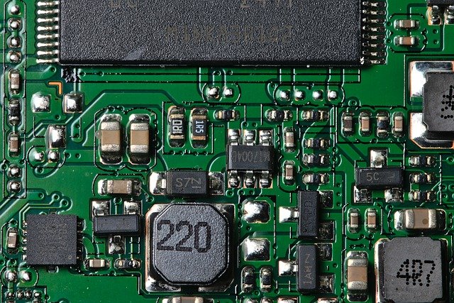
Ball grid array is a type of surface mount packaging. BGA is used for microprocessors.
We can do fill via with conductive ink and plate over or fill via with non-conductive ink and plate over.
Minimum 16-18mil hole size required with 10-12 mil spacing to do this process.
We can do selective hard gold plating upto 40-50u”.